Ibm at hot chips: what’s next for power
With processor, memory as well as networking technologies all racing to complete to have an ailing Moore’s law, the time of the heterogeneous datacenter is well going ahead, and IBM is positioning its chips is the air traffic controller in the center from it all. Which was our prime-level takeway in our interview with IBM Power architects Shaun Stuecheli and Bill Starke at Hot Chips now.
The accomplished engineers were in the 30th iteration of Hot Chips to pay attention to the Power9 scale-up chips and servers, they also provided information on approaching developments within the roadmap, together with a new buffered memory system appropriate for scale-out processors.
 Source: IBM slide (Hot Chips 30)
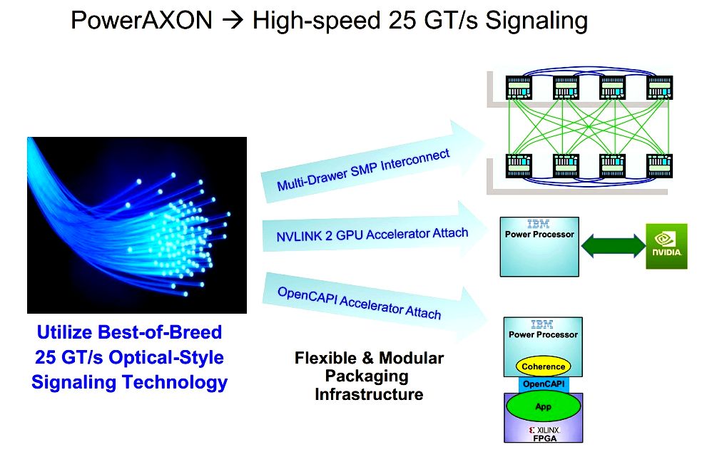
Getting launched both scale-out and scale-up Power9s, IBM has become focusing on another P9 variant with “advanced I/O,” featuring IBM’s 25 GT/s PowerAXON signaling technology with upgraded OpenCAPI and NVLink protocols, along with a new open standard for buffered memory.
AXON is definitely an inspired appellation the Power engineering team created and also the IBM marketing team signed off on. The A and X are designations for IBM’s SMP buses – X links take presctiption-module along with a links are from the O and N are a symbol of OpenCAPI and NVLINK, correspondingly. The convenient acronym could be fine at this, but aligning with IBM’s penchant for cognitive computing, axons would be the brain’s signalling devices, allowing neurons to speak, which means you could say, as Witnix founder and former Harvard HPC guy James Cuff did, that AI generally is “built directly into the wire.”
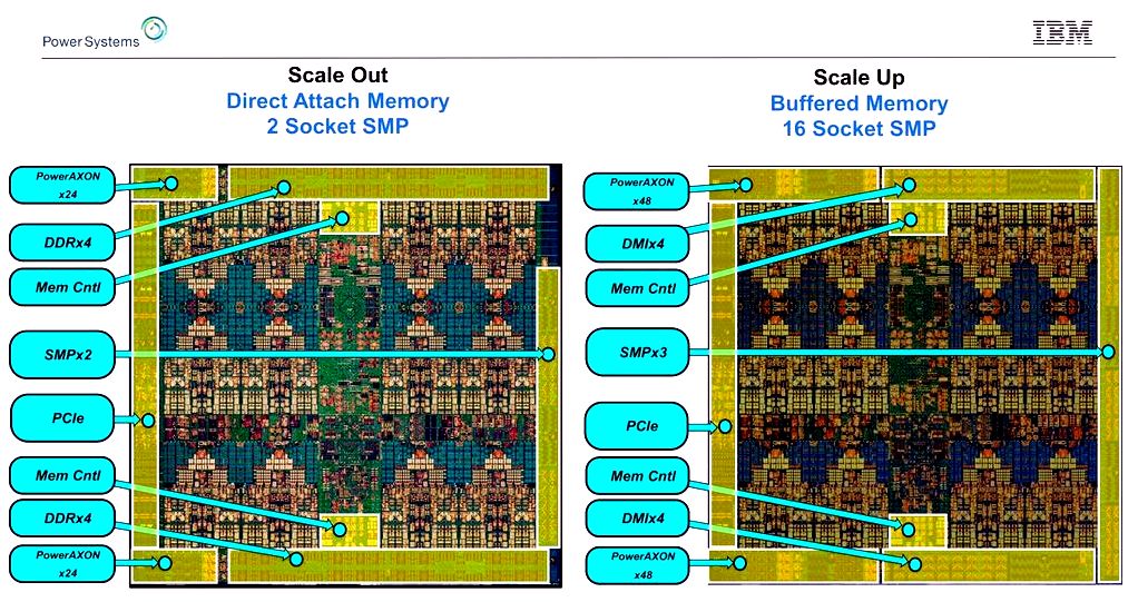 You can observe on these annotated Power9 die shots how going from the DDR memory controller to some redrive memory controller on and on to smaller sized PHYs enabled IBM to double the amount of AXON lanes.
“The PowerAXON concept provides for us lots of versatility,” stated Stuecheli. “One nick could be deployed to become a big SMP, it may be deployed to speak to plenty of GPUs, it may speak with a mixture of FPGAs and GPUs – that’s really our goal here’s to construct a processor that may then be customized toward these domain specific applications.”
Because of its future products, IBM is concentrating on plenty of lanes and a lot of frequency. Its Power10 roadmap incorporates 32 GT/s signalling technology that can run in 50 GT/s mode.
The concept that IO is composable is exactly what OpenCAPI and PowerAXON are only for – and today IBM is getting this same ethos to memory through the introduction of a wide open standard for buffered memory, appropriately known as OpenCAPI memory.
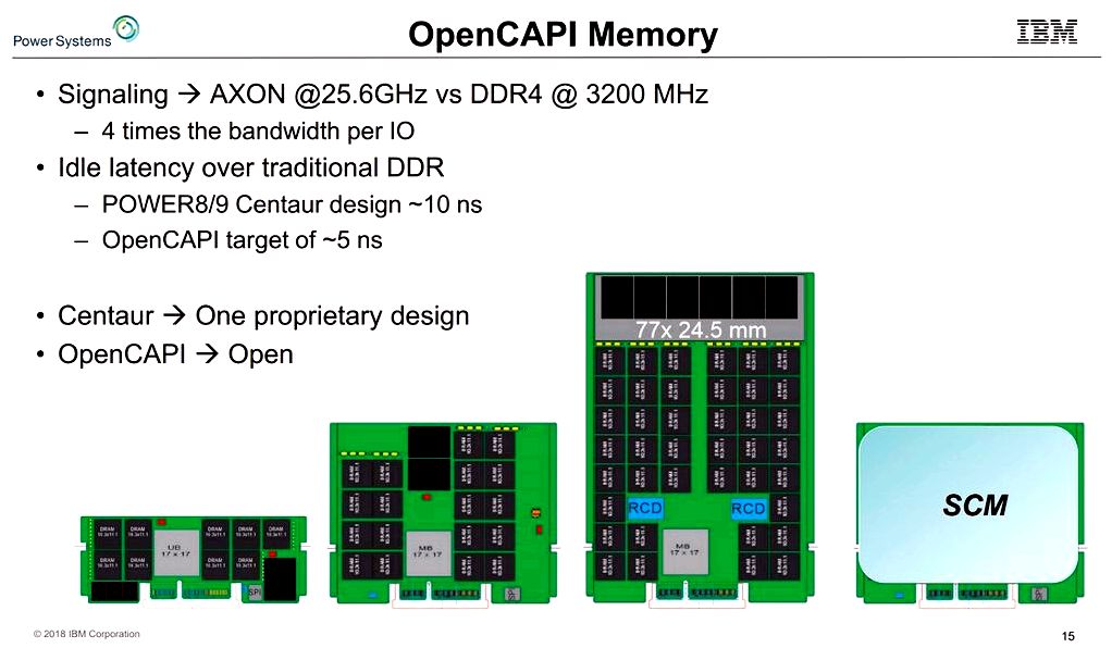
With Power8 and Power9, the chips designed for scale-out boxes support direct-attached memory, as the scale-up variants, meant for machines using more than two sockets, employ buffered memory. The buffered memory system puts DRAM chips right alongside IBM’s Centaur buffer nick (see figure below-right), enabling a lot of DDR channels to become funneled into one processor over SERDES. The agnostic interface hides the precise memory technology that’s around the DIMM in the processor, therefore the processor could work with different types of memory. This decoupling of memory technology in the processor technology implies that, for instance, enterprise customers upgrading from Power8 to Power9 will keep their existing DDR4 DRAM DIMMs.
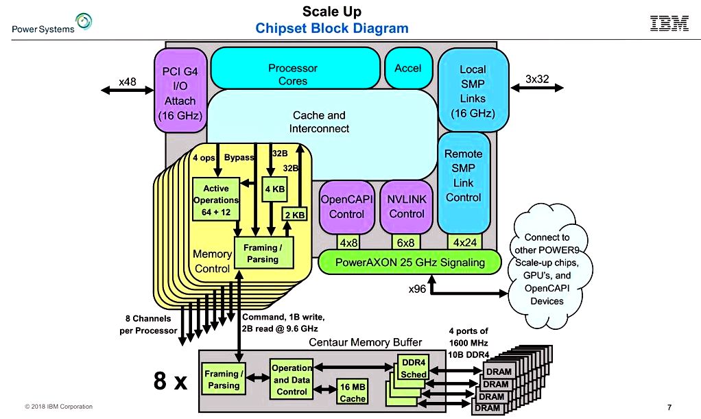 Power9 Scale Up chipset block diagram
Stuecheli shared the current buffered memory system (on Power8 and Power9 SU chips) adds a latency of roughly 10 nanoseconds when compared with direct attached. This minimal overhead was accomplished “through careful framing from the packets because they go over the SERDES and bypasses within the DDR scheduling,” stated Stuecheli.
As the Centaur-based approach is enterprise-focused, IBM wanted to give the same buffered memory in the scale-out products. They are intending to introduce this capacity being an open standard within the third (and presumably final) Power9 variant, going to be out in 2019. “We’ve been dealing with JEDEC to construct memory DIMMs based on a skinny buffer design,” stated Stuecheli. “If you possess an accelerator and also you don’t like getting that big costly DDR PHY on you and it desire to use just traditional SERDES to speak to memory that can be done using the new standardized memory interface we’re building,” he told the crowd at Hot Chips. The interface spans from 1U small memory form factors completely as much as big tall DIMMs. The goal is with an agnostic interface that attaches to a number of memory types into it, whether that’s storage-class memory, or high bandwidth, low capacity memory.
As the latency add was 10 nanoseconds around the proprietary design (with one port likely to four DDR ports having a 16MB cache lookup), the brand new buffer IBM is building is really a single port design having a single interface. It’s a significantly smaller sized nick with no cache, and IBM thinks it may reduce this latency to five nanoseconds. Stuecheli stated that company-run simulations with loaded latency demonstrated it doesn’t take much load whatsoever before supplying reduced latency than the usual direct-attached solution.
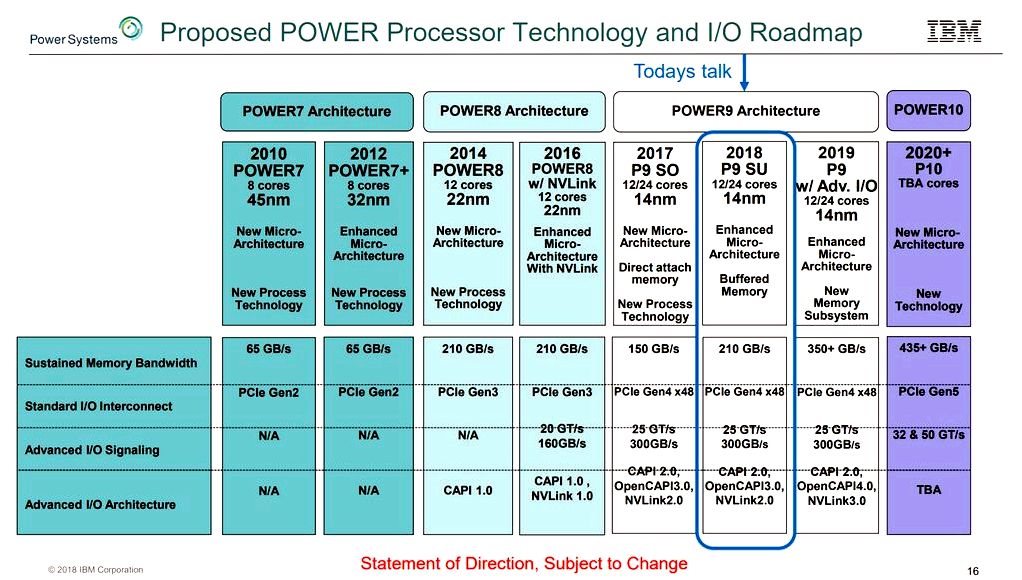
The roadmap shows the anticipated rise in memory bandwidth because of the brand new memory system. In which the Power9 SU nick offers 210 GB/of memory bandwidth (and Stuecheli states it’s really nearer to 230 GB/s), the following Power9 derivative nick, using the new memory technology, will manage to deploying 350 GB/s per socket of bandwidth, based on Stuecheli.
“If you’re in HPC and disappointed inside your bytes-per-flop ratio, that’s a reasonably large improvement,” he stated, adding “we’re taking that which was basically the Power10 memory subsystem and applying that in Power9.” With Power10 getting in DDR5, IBM expects to exceed 435 GB/s sustained memory bandwidth.
IBM believes that her right method of push past DDR limitations. “When you consider Moore’s law type of winding lower, slowing lower, you consider single-ended signaling with DDR memory slowing lower,” Bill Starke stated inside a pre-briefing. “This composable system construct [that IBM is architecting] is enabling a proliferation more heterogeneity in compute technology, plus a wider variation of memory technologies, all within this composable plug-and-play, put-it-together-how-you-want way where it’s some facts about the big high-bandwidth low-latency switching infrastructure.”
“With the versatility from the attach around the memory side as well as on the compute acceleration side, it truly boils lower to considering the CPU nick because this big switch,” Stuecheli adopted, “this big data switch that’s only one big pile of bandwidth connectivity that’s enabling any type of memory to speak to any type of acceleration, also it all plumbs right beyond the effective general-purpose processor cores, so you’re pulling that whole compute estate together.”
HPC analyst Addison Snell (Chief executive officer of Intersect360 Research) came from Tuesday’s Hot Chips talk to a good impression from the Power play. “IBM’s presentation at Hot Chips underscored two major styles,” Snell commented by email. “One, Power9 has excellent memory bandwidth and gratifaction. Two, it’s a great platform for attaching accelerators or co-processors. It’s a strange statement of direction, but perhaps a visionary one, basically saying a processor isn’t about computation by itself, but instead sturdy feeding data with other computational elements.”
Resourse: https://hpcwire.com/2018/08/23/ibm-at-hot-chips-whats-next-for-power/

