Wide i/o: memory interface standard for 3d ic – semiconductor engineering
Description
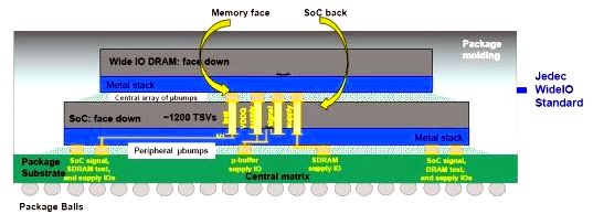
Wide I/O is really a memory interface standard for 3D IC created by JEDEC (JESD229). The fundamental concept is by using a really many pins, because both versions is comparatively slow but low powered. These concepts wouldn’t be feasible for a PCB kind of interconnect due to the pin limitations of individuals environments and also the power and signal integrity issues connected with passing signals across a PCB. With stacked dies, the amount of interconnects turns into a lot bigger since they’re not restricted to the periphery from the device. Additionally, distances could be under track lengths across nick, rather being between thin die stacked vertically (50-100um). This reduces capacitance and therefore power consumption.
This interface was initially standardized by JEDEC in The month of january 2012 It specifies 4 128-bit channels to DRAM running at 200MHz using single data rate technology. It creates a complete bandwidth of 100Gb/S
Wide I/O 2 August 2014
Description
Wide I/O is really a memory interface standard for 3D IC created by JEDEC (JESD229). The fundamental concept is by using a really many pins, because both versions is comparatively slow but low powered. These concepts wouldn’t be feasible for a PCB kind of interconnect due to the pin limitations of individuals environments and also the power and signal integrity issues connected with passing signals across a PCB. With stacked dies, the amount of interconnects turns into a lot bigger since they’re not restricted to the periphery from the device. Additionally, distances could be under track lengths across nick, rather being between thin die stacked vertically (50-100um). This reduces capacitance and therefore power consumption.
This interface was initially standardized by JEDEC in The month of january 2012 It specifies 4 128-bit channels to DRAM running at 200MHz using single data rate technology. It creates a complete bandwidth of 100Gb/S
Wide I/O 2 August 2014
Wide I/O 2 provides four occasions the memory bandwidth (as much as 68GBps) from the previous form of the conventional, but at lower power consumption (better bandwidth/Watt) using the switch to 1.1V supply current. From the packaging perspective, the Wide I/O 2 die is enhanced to stack on the top of the system on nick (SOC) to reduce power consumption and footprint.
The conventional defines interfaces for 8 Gb through 32 Gb SDRAM devices with 4 or 8 64-bit wide channels using direct nick-to-nick attach means of between 1 and 4 memory devices along with a controller/buffer device. The WideIO2 architecture is definitely an evolution from the WIO architecture to allow bandwidth scaling with capacity.
Resourse: https://semiengineering.com/understanding_centers/standards-laws and regulations/standards/wide-io-2/

