Various kinds of ram (ram ) – geeksforgeeks
RAM(Ram) is part of computer’s Primary Memory that is directly accessible by CPU. RAM can be used to Read data in it that is utilized by CPU at random. RAM is volatile anyway, this means when the power beeps, the stored details are lost. RAM can be used to keep the information that’s presently processed through the CPU. The majority of the programs and knowledge which are modifiable are kept in RAM.
Integrated RAM chips can be found in two form:
- SRAM(Static RAM)
- DRAM(Dynamic RAM)
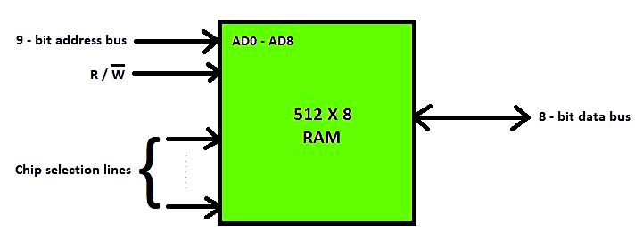
The block diagram of RAM nick is offered below.
SRAM
The SRAM recollections contain circuits able to retaining the stored information as lengthy because the power is used. Which means this kind of memory requires constant power. SRAM recollections are utilized to build Cache Memory.
SRAM Memory Cell: Static recollections(SRAM) are recollections that contain circuits able to retaining their condition as lengthy as power is on. Thus this kind of recollections is known as volatile recollections. The below figure shows a cell diagram of SRAM. A latch is created by two inverters connected as proven within the figure. Two transistors T1 and T2 can be used for connecting the latch with two bit lines. The objective of these transistors would be to behave as switches that may be opened up or closed underneath the charge of the term line, that is controlled through the address decoder. Once the word lines are at -level, the transistors are switched off and also the latch remains its information. For instance, the cell reaches condition 1 when the logic value at point A is 1 and also at point B is . This condition is retained as lengthy because the word lines are not activated.
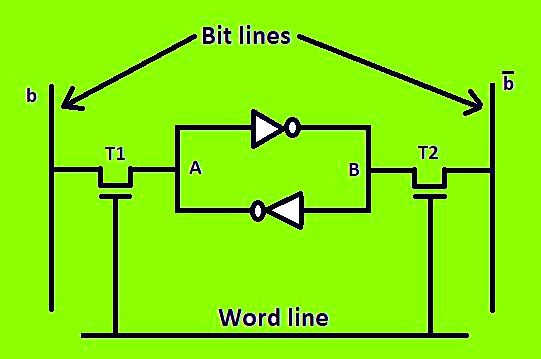
For Read operation, the term lines are activated through the address input towards the address decoder. The activated word line closes both transistors (switches) T1 and T2. Then your bit values at points A and B can transmit for their particular bit lines. A feelingOrcreate circuit in the finish from the bit lines transmits the output towards the processor.
For Write operation, the address presented to the decoder activates the term line to shut both switches. Then your bit value that to become written in to the cell is supplied with the sense/write circuit and also the signals in bit line is then kept in the cell.
DRAM
DRAM stores the binary information by means of electric charges that put on capacitors. The stored info on the capacitors have a tendency to lose during a period of some time and thus the capacitors should be periodically recharged to retain their usage. The primary memory is usually comprised of DRAM chips.
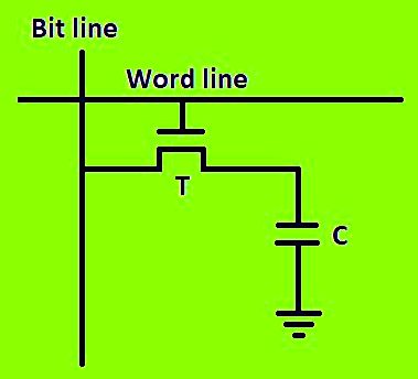
DRAM Memory Cell: Though SRAM becomes manifest pretty quickly, but it’s costly due to its every cell requires several transistors. Relatively less costly RAM is DRAM, because of the utilization of one transistor and something capacitor in every cell, as proven within the below figure., where C may be the capacitor and Its the transistor. Details are kept in a DRAM cell by means of electric power charge on the capacitor which charge must be periodically recharged.
For storing information within this cell, transistor Its switched on as well as an appropriate current is used towards the bit line. This will cause a known quantity of charge to become kept in the capacitor. Following the transistor is switched off, because of the property from the capacitor, it begins to discharge. Hence, the data kept in the cell could be read properly only if it’s read prior to the charge around the capacitors drops below some threshold value.
Kinds of DRAM
You will find mainly 5 kinds of DRAM:
-
Asynchronous DRAM (ADRAM): The DRAM described above may be the asynchronous type DRAM. The timing from the memory system is controlled asynchronously. A specialized memory controller circuit generates the required control signals to manage the timing. The CPU must look at the delay within the response from the memory.
-
Synchronous DRAM (SDRAM): These RAM chips’ access speed is directly synchronized using the CPU’s clock. With this, the memory chips remain ready for operation once the CPU expects these to prepare yourself. These recollections operate in the CPU-memory bus without imposing wait states. SDRAM is commercially accessible as modules incorporating multiple SDRAM chips and developing the needed convenience of the modules.
-
Double-Data-Rate SDRAM (DDR SDRAM): This faster form of SDRAM performs its operations on edges from the clock signal whereas a typical SDRAM performs its operations around the rising fringe of the time signal. Given that they transfer data on edges from the clock, the information transfer rates are bending. To gain access to the information at high rate, the memory cells are organized into two groups. Each group is utilized individually.
-
Rambus DRAM (RDRAM): The RDRAM supplies a high bandwith rate more than a narrow CPU-memory bus. It uses various speedup mechanisms, like synchronous memory interface, caching within the DRAM chips and incredibly fast signal timing. The Rambus data bus width is 8 or 9 bits.
-
Cache DRAM (CDRAM): This memory is really a special type DRAM memory by having an on-nick cache memory (SRAM) that functions like a high-speed buffer for that primary DRAM.
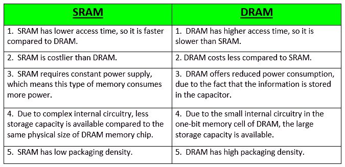
Distinction between SRAM and DRAM
Below table lists a few of the variations between SRAM and DRAM:
Resourse: https://geeksforgeeks.org/different-types-ram-random-access-memory/

