Hyperram: utilizing a hyperbus memory interface nick
About latency and synchronization is going to be discussed below.
Data exchange using the device happens by means of transactions: the actual will arrange the nick-select, supplies a clock signal, issues control bytes, waits for many cycles, communicates, stops synchronization, and de-selects the nick-select.
Within the first three cycles, the host transmits 6 transaction control bytes (COMMAND-ADRESS or CA ). Without entering details, simply list the parameters:
- Transaction type: read or write.
- Address space: memory or control registers.
- The kind of write / read sequence: straight line (straight line) or batch (burst).
- The address for beginning memory access in posts and rows.
Since memory cells can’t be recharged throughout a data exchange transaction, limitations are enforced around the duration of merely one transaction (transaction duration) and also the delay together (initial latency).
Concurrently using the change in the CA, the memory wears the RWDS line an indicator of latency: the number of clock cycles should be anxiously waited before issuing data for writing, or receiving data for studying. The need for the amount of cycles we gain knowledge from the control register. This value is dependent upon the memory individually, with respect to the clocking frequency. If RWDS is at “0”, we predict the needed quantity of cycles once, if at “1” – two times. By setting the unit registers, you are able to set the memory to continually focus on a dual delay interval, and hang the amount of ticks not the same as the default value (however this value shouldn’t be under the initial).
Inside a write transaction, after awaiting the needed quantity of ticks, the host puts write data towards the bus:
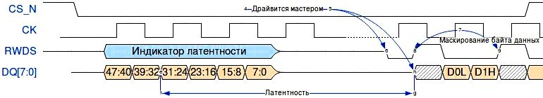
Write transaction
The information is taken through the memory on fronts from the sync signal, correspondingly, the information are positioned within the output DDR register with a clock shifted 270 levels. The RWDS signal within the bandwith process masks the bytes that shouldn’t be altered through the memory within the recording process. When writing a thing towards the control registers, it should be issued soon after the SA with no delay.
Inside a read transaction, the information is occur memory:
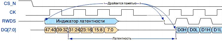
Read transaction
Data changes around the bus are synchronized with edges from the RWDS signal. It’s also wise to remember the data generated through the memory is synchronized through the RWDS signal around the front. Consequently, for proper studying, RWDS ought to be shifted by 90 levels:
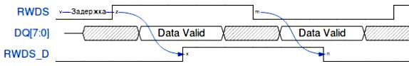
RWDS signal delay in accordance with data signal
Data studying / studying begins in the address specified by the CA. The address with every received / issued word is incremented by 2. The transaction ends once the clock signal stops and also the chipset deassert stops.
We note several options that come with the job. First, once the address covers the utmost value, data begins to be output / recorded within an indefinite manner. Therefore, you shouldn’t connect to the memory of transactions that overflow the address counter. Second, the microcircuit limits the time period of the transaction, since periodic recharging from the memory elements is needed. Maximum durations rely on temperature and therefore are succumbed the specs. Within the toughest situation, in a single transaction in a speed of 166 MHz, read / write a bit more than 300 bytes.
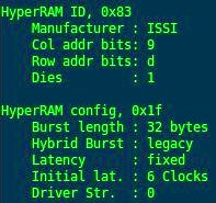
The unit has two registers: information and configuration. The data register gives us details about the maker and kind of device (HyperRAM / HyperFLASH), the amount of rows, posts and crystals from the device. The configuration register enables configuring the output impedance, packet length within the packet data access mode, latency type (constant / variable), as well as enables you to definitely set the delay value and set the unit into low power consumption mode (Deep Power Lower).
Initially glance, the issue may arise: how do you read the need for the configuration register with details about the delay, if the delay is unknown during the time of studying? With this it’s important to take into consideration the data output is synchronized through the memory across the RWDS line. And, actually, the particular worth of the delay isn’t taken into consideration anywhere, because the data capture plan is source-synchronous. As well as in the transaction record, on the other hand, we have to count the cycles before issuing data, with respect to the worth of latency and also the condition from the RWDS signal.
Here’s a good example of parsing the of the configuration registers:
findings
Generally, the memory interface HyperBUS left only enjoyable impressions. Around the FPGA, dealing with it’s quite simple and also the developed module is not resource-intensive. The only real current drawback may be the limited selection of microcontrollers with HyperBUS. Therefore we will wait for a interface support by a lot of vendors and distinctively carry it out within our (as well as in your 🙂 future projects.
About latency and synchronization is going to be discussed below.
Data exchange using the device happens by means of transactions: the actual will arrange the nick-select, supplies a clock signal, issues control bytes, waits for many cycles, communicates, stops synchronization, and de-selects the nick-select.
Within the first three cycles, the host transmits 6 transaction control bytes (COMMAND-ADRESS or CA ). Without entering details, simply list the parameters:
- Transaction type: read or write.
- Address space: memory or control registers.
- The kind of write / read sequence: straight line (straight line) or batch (burst).
- The address for beginning memory access in posts and rows.
Since memory cells can’t be recharged throughout a data exchange transaction, limitations are enforced around the duration of merely one transaction (transaction duration) and also the delay together (initial latency).
Concurrently using the change in the CA, the memory wears the RWDS line an indicator of latency: the number of clock cycles should be anxiously waited before issuing data for writing, or receiving data for studying. The need for the amount of cycles we gain knowledge from the control register. This value is dependent upon the memory individually, with respect to the clocking frequency. If RWDS is at “0”, we predict the needed quantity of cycles once, if at “1” – two times. By setting the unit registers, you are able to set the memory to continually focus on a dual delay interval, and hang the amount of ticks not the same as the default value (however this value shouldn’t be under the initial).
Inside a write transaction, after awaiting the needed quantity of ticks, the host puts write data towards the bus:
Write transaction
The information is taken through the memory on fronts from the sync signal, correspondingly, the information are positioned within the output DDR register with a clock shifted 270 levels. The RWDS signal within the bandwith process masks the bytes that shouldn’t be altered through the memory within the recording process. When writing a thing towards the control registers, it should be issued soon after the SA with no delay.
Inside a read transaction, the information is occur memory:
Read transaction
Data changes around the bus are synchronized with edges from the RWDS signal. It’s also wise to remember the data generated through the memory is synchronized through the RWDS signal around the front. Consequently, for proper studying, RWDS ought to be shifted by 90 levels:
RWDS signal delay in accordance with data signal
Data studying / studying begins in the address specified by the CA. The address with every received / issued word is incremented by 2. The transaction ends once the clock signal stops and also the chipset deassert stops.
We note several options that come with the job. First, once the address covers the utmost value, data begins to be output / recorded within an indefinite manner. Therefore, you shouldn’t connect to the memory of transactions that overflow the address counter. Second, the microcircuit limits the time period of the transaction, since periodic recharging from the memory elements is needed. Maximum durations rely on temperature and therefore are succumbed the specs. Within the toughest situation, in a single transaction in a speed of 166 MHz, read / write a bit more than 300 bytes.
The unit has two registers: information and configuration. The data register gives us details about the maker and kind of device (HyperRAM / HyperFLASH), the amount of rows, posts and crystals from the device. The configuration register enables configuring the output impedance, packet length within the packet data access mode, latency type (constant / variable), as well as enables you to definitely set the delay value and set the unit into low power consumption mode (Deep Power Lower).
Initially glance, the issue may arise: how do you read the need for the configuration register with details about the delay, if the delay is unknown during the time of studying? With this it’s important to take into consideration the data output is synchronized through the memory across the RWDS line. And, actually, the particular worth of the delay isn’t taken into consideration anywhere, because the data capture plan is source-synchronous. As well as in the transaction record, on the other hand, we have to count the cycles before issuing data, with respect to the worth of latency and also the condition from the RWDS signal.
Here’s a good example of parsing the of the configuration registers:
findings
Generally, the memory interface HyperBUS left only enjoyable impressions. Around the FPGA, dealing with it’s quite simple and also the developed module is not resource-intensive. The only real current drawback may be the limited selection of microcontrollers with HyperBUS. Therefore we will wait for a interface support by a lot of vendors and distinctively carry it out within our (as well as in your 🙂 future projects.
Resourse: https://weekly-geekly.github.io/articles/344966/

